Reset needs time!
I found an interesting and inexpensive (about 10-12€) EC1204B DIY electronic clock kit on aliexpress. There was not much documentation about the kit, but there is enough on the net. Cristian Copcea has gathered a lot of documentation on this kit and even provides an alternative open-source firmware. Schematic is here. Quite an interesting design with an older 8-bit Atmel AT89S52 CPU, external 1-wire DS1302 clock and DS18B20 temperature sensor, matrix-driven LEDs, LED display and USB power. All transistors are PNP, perhaps they were a tiny bit cheaper.
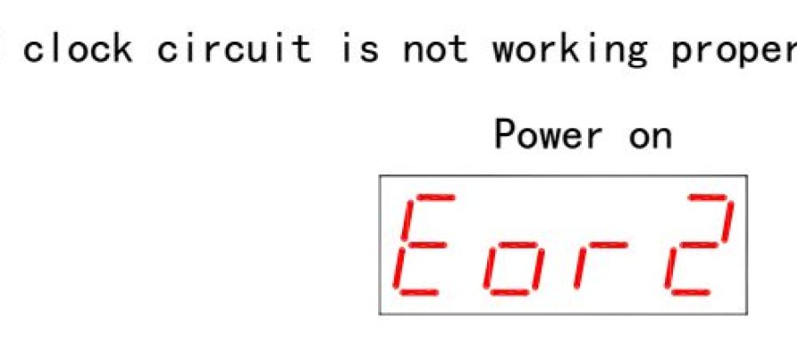
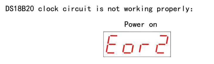
We soldered the clock together with my daughter Alina. It was fun soldering SMD and THT, but all we got was an "Eor2" error and an ugly noise, as we did with another kit. It seems to be a problem with the DS18B20 temperature sensor.
 I traced its DQ line with an excelent Saleae Logic 8 logic analyser. I saw only one pulse:
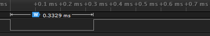
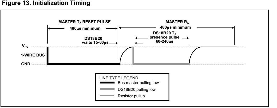
According to the DS18B20 datasheet the reset pulse is obviously too short. Reset needs time:
One solution is to exchange the Y1 12MHz quartz for a slower one. I had 8 MHz quartz lying around and it worked, except for the power-on reset, so I have to press RST for the clock to start. Reset needs time. Perhaps C5 needs to be increased to say 10 uF or C3 and C4 are too small (datasheet mentions 30 pF +/- 10 pF).
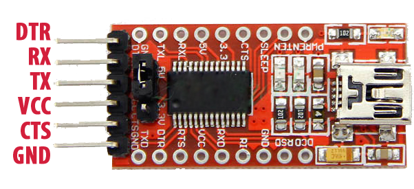
Another solution is to reprogram the chip, so I took an unmodified clock, a cheap FT232 breakout board and FT232-enabled version of avrdude by Mr. Suz.
I added FT232 and AT89S52 (note the inverted reset =~4 for this CPU) to avrdude.conf based on the above link and this discussion and contribution by Joy Shukla. But avrdude -c ftdi -p AT89S52 -P ft0 -n is failing for now, no pulses on MISO line.
Reset needs more time? I have to check.
#------------------------------------------------------------
# AT89S52
#------------------------------------------------------------
part
    id               = "8052";
    desc             = "AT89S52";
    signature        = 0x1E 0x52 0x06;
    chip_erase_delay = 500000;
    pgm_enable       = "1 0 1 0  1 1 0 0    0 1 0 1  0 0 1 1",
                       "x x x x  x x x x    x x x x  x x x x";

    chip_erase       = "1 0 1 0  1 1 0 0    1 0 0 x  x x x x",
                       "x x x x  x x x x    x x x x  x x x x";

    timeout      = 200;
    stabdelay      = 100;
    cmdexedelay      = 25;
    synchloops      = 32;
    bytedelay      = 0;
    pollindex      = 3;
    pollvalue      = 0x53;
    predelay      = 1;
    postdelay      = 1;
    pollmethod      = 0;

    memory "flash"
        size            = 8192;
        paged           = no;
        min_write_delay = 4000;
        max_write_delay = 9000;
        readback_p1     = 0xff;
        readback_p2     = 0xff;
        read            = "  0   0   1   0    0   0   0   0",
                          "  x   x   x a12  a11 a10  a9  a8",
                          " a7  a6  a5  a4   a3  a2  a1  a0",
                          "  o   o   o   o    o   o   o   o";

        write           = "  0   1   0   0    0   0   0   0",
                          "  x   x   x a12  a11 a10  a9  a8",
                          " a7  a6  a5  a4   a3  a2  a1  a0",
                          "  i   i   i   i    i   i   i   i";
   mode      = 0x21;
   delay      = 12;
      ;

    memory "signature"
        size            = 3;
        read            = "0  0  1  0   1  0  0  0   x  x  x  0   0  0 a1 a0",
                          "0  0  0  0   0  0  0  0   o  o  o  o   o  o  o  o";
      ;
  ;

#PIN NO.     DATA LINE
#   0           TXD
#   1           RXD
#   2           RTS
#   3           CTS
#   4           DTR
#   5           DSR
#   6           DCD
#   7           RI
programmer
  id    = "ftdi";
  desc  = "FT232R BitBang Programmer";
  type  = ft245r;
  miso  = 1;  # RxD
  sck   = 2;  # RTS
  mosi  = 0;  # TxD
  reset =~4;  # DTR

  #miso  = 5; # DSR
  #sck   = 4; # DTR
  #mosi  = 6; # DCD
  #reset = 7; # RI
;
Patch by Shigemaru Nishiyama
In January 2018 I got a message from Shigemaru Nishiyama, who managed to read back and patch the original clock firmware. His code is here.
I was wondering how he did it. He said he was looking for byte 90h, as DS18B20 is on P1.0 and 90h is its bit address in 8051 (google for 8051 memory map). Then he increased the delay constants. Unfortunately he does not have an original file for a clean delta. I looked with a disassembler, and found what looks like a reset routine, which I suppose he has patched:
seg000:1A77             reset_ds18b20:                          ; CODE XREF: seg000:seg000_BE3
seg000:1A77 C2 90                   clr     FSR_90.0
seg000:1A79 7F 2C                   mov     R7, #0x2C ; <== suppose this constant has been doubled
seg000:1A7B 7E 00                   mov     R6, #0
seg000:1A7D 12 1B 12                lcall   delay           ; count in R6:R7
seg000:1A80 D2 90                   setb    FSR_90.0
seg000:1A82 7F 03                   mov     R7, #3
seg000:1A84 7E 00                   mov     R6, #0
seg000:1A86 12 1B 12                lcall   delay           ; count in R6:R7
seg000:1A89 A2 90                   mov     C, FSR_90.0
seg000:1A8B 92 0A                   mov     RAM_21.2, C
seg000:1A8D A2 0A                   mov     C, RAM_21.2
seg000:1A8F 22                      ret
... and what looks like a read routine:
seg000:19E2             read_ds18b20:                           ; CODE XREF: seg000_16C9+1A
seg000:19E2 AD 07                   mov     R5, RAM_7
seg000:19E4 7B 08                   mov     R3, #8
seg000:19E6
seg000:19E6             ds18b20_b:                              ; CODE XREF: read_ds18b20+18
seg000:19E6 C2 90                   clr     FSR_90.0
seg000:19E8 ED                      mov     A, R5
seg000:19E9 13                      rrc     A
seg000:19EA 92 90                   mov     FSR_90.0, C
seg000:19EC 7F 03                   mov     R7, #3
seg000:19EE 7E 00                   mov     R6, #0
seg000:19F0 12 1B 12                lcall   delay           ; count in R6:R7
seg000:19F3 D2 90                   setb    FSR_90.0
seg000:19F5 ED                      mov     A, R5
seg000:19F6 A2 E7                   mov     C, FSR_E0.7
seg000:19F8 13                      rrc     A
seg000:19F9 FD                      mov     R5, A
seg000:19FA DB EA                   djnz    R3, ds18b20_b
seg000:19FC 22                      ret